|
|
II-INFORMATIK3 WS04
|
In der heutigen --abschliessenden-- Vorlesung soll das Thema Prozessorarchitektur und Optimierungsstrategien unter der speziellen Rücksicht betrachtet werden, dass das Anwendungsszenarium ein eingebettetes (embedded) System verlangt, das zudem noch ein Realzeitsystem (real time system) sein soll. Zusätzlich soll festgelegt werden, dass als Realzeitsystem das noch sehr junge RTAI (:= Real Time Application Interface) der technischen Universität von Mailand gewählt werden soll, das im Verbund mit Linux arbeitet.
Diese Annahmen sind im technischen Anwendungsbereich sehr realistisch, da der Anteil von eingebetteten Systeme gerade im technischen Bereich sehr hoch ist. Ausserdem hat gerade in den letzten Jahren Linux als eingebettetes System zweistellige Wachstumsraten und ist auf dem besten Weg, zum führenden Standard für eingebettete Systeme zu werden.
Stellt man sich die Frage, welche CPUs tatsächlich im industriellen Bereich zum Einsatz kommen, dann sind es vor allem die folgenden CPU-Architekturen:
x86-CPUs
Power PCs
ARM-CPUs
XScale-CPUs PXA255/270
MSP430
Während die x86-CPUs sich in ihren verschiedenen Versionen durch eine durchgängig einheitliche Memorymap und ein einheitliches BIOS auszeichnen, variiert dies bei den anderen CPUs vollständig. Doch haben diese anderen CPUs gegenüber den x86-CPUs den Vorteil deutlich geringerer Leistungsaufnahme. Erst die neuen XScale-CPUs von Intel, die auf der ARM-Architektur aufsetzen, können mit der ARM-CPU bezüglich Leistungsverbrauch mithalten. Eine Spizenstellung hinsichtlich Kleinheit der Abmessung und geringem Leistungsverbrauch nimmt aber zur Zeit die CPU MSP430 von Texas Instruments ein.
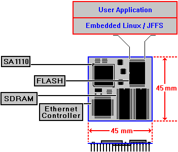
Als Standardanwendung nehmen wir das 1-Chip-Board DIL/NetPC PNP/1110 der Firma SSV Embedded Systems (Hannover). Es vereint auf kleinstem Raum (siehe nachfolgendes Bild) eine strong-ARM CPU mit Flashrom, SDRAM, Ethernetkontroller und diversen Schnittstellen.
DIL/NetPC PNP/1110 |
||
|---|---|---|
| |
|
|
In der Erläuterung zu diesem Board heisst es weiter:
The DIL/NetPC PNP/1110 provides a very compact Intel 206 MHz SA-1110 StrongARM-based low power embedded controller with TCP/IP stack and web server for network-based or mobile embedded user interface applications. The DIL/NetPC offers the footprint of a standard 169-pin PGA socket with 2.54mm centers and all the hardware and software features necessary to add high-speed networking capabilities to any product design. The DIL/NetPC PNP/1110 was developed specifically for industrial user interface products that need to be driven by high-resolution graphic LCD with minimum development costs.
The PNP/1110 comes as ready-to-run system for GUI (graphical user interfaces) applications. Just connect a high-resolution LCD and run the pre-installed Linux-based X server, that is all. The use of the PNP/1110 will allow you to realize a substantial time and costs savings over other chip- or board-based approaches. Currently, there is no other solution with more development time savings on the market. There is also no faster Time-to-Market for your industrial GUI-based product.
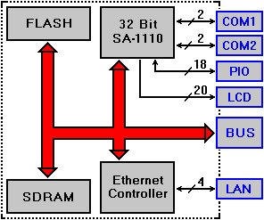
To interface the PNP/1110 with existing devices and equipment, the PNP/1110 offers two asynchronous serial RS232C interfaces with TTL levels and handshake signals (COM1/COM2 - 16550 compatible), 18-bit general purpose high-speed parallel I/Os and a 32-bit high-speed expansion bus with interrupt inputs and chip select outputs. There are two ways for PNP/1110 integration: 1. Adapt the PNP/1110 to your existing product. Use the existing I/Os within your product to communicate with the PNP/1110. 2. Use the PNP/1110 to control and monitor the hardware of your existing product. This might enable you to replace your existing controller entirely. In a new product design, the PNP/1110 can be the main controller. Additional I/Os are driven by the 32-bit high-speed expansion bus.
The on-board FLASH memory provides storage for the PNP/1110 operating system with TCP/IP stack and embedded web server as well as OEM applications and data. The FLASH memory is in-system programmable over JTAG, serial and the Ethernet interface. The boot block of the FLASH memory is only in-system programmable over the JTAG interface through a special cable attached to a PC parallel port. For all other FLASH blocks, you can use also a high-speed serial connection through the PNP/1110 COM1 port or the 10/100 Mbps Ethernet interface for in-system programming (networking version only). The PNP/1110 in-system programming was developed for OEM application software, operating system downloads (i.e. upgrade from embedded Linux to eCos) and data download and to make it easier to update the on-board FLASH content in the field.
DIL/NetPC PNP/1110: Key Features
DIL/NetPC PNP/1110: Description
The PNP/1110 is build around the Intel StrongARM SA-1110 32-bit RISC microcontroller running with 206 MHz. The SA-1110 has a large instruction and data cache, memory-management unit (MMU), and read/write buffers. The SA-1110 offers high-performance processing power with up to 235 Dhrystone 2.1 MIPS. The SA-1110 CPU core implements the ARM V4 architecture as defined in the ARM Architecture Reference Manual. The SA-1110 provides a complete set of internal peripherals. There are multiple serial communication channels, general-purpose I/O ports, timers, interrupt control, reset control, LCD controller, PCMCIA interface logic, and power management functions.
The external main components around the Intel StrongARM SA-1110 32-bit RISC microcontroller on the PNP/1110 are one FLASH chip with 16 MBytes, two 32 MByte SDRAM chips (64 MByte total SDRAM), and one 10/100 Mbps Ethernet LAN controller with 10BASE-T and 100BASE-TX physical layer interface (PNP/1110 networking version only). The FLASH stores the hardware setup code, the SSV Flash Loader, the boot loader, operating system, and OEM applications. The SDRAM access and the refresh operation is driven by the SA-1110 integrated SDRAM controller.
The PNP/1110 10/100 Mbps Ethernet controller is a SMSC LAN91C111 single chip MAC+PHY. This highly-integrated Ethernet LAN controller of the PNP/1110 networking version includes 8 KByte internal memory for receive and transmit FIFO buffers, a IEEE 802.3/802.3u Ethernet MAC engine, and internal 10BASE-T and 100BASE-TX transmit and receive filters. The SMSC LAN91C111 supports full-duplex switched Ethernet operation and auto negotiation for 10 and 100 Mbps. For the PNP/1110 LAN integration, the PHY interface needs only a external low-cost isolation transformer.
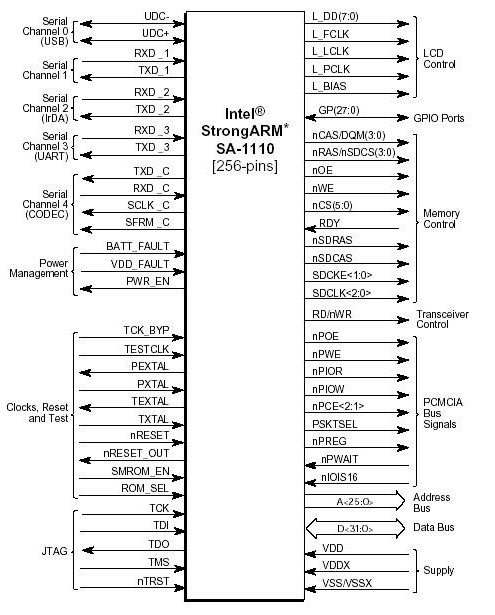
The mechanical interface between the PNP/1110 and existing devices and equipment is a JEDEC 169-pin PGA connector with 2.54mm centers. This allows the direct integration to a standard 169-pin PGA socket. The 169 pins in total are used for 3.3 volt power supply (32 pins, including Vcc, GND, Vbat ), Reset in and out (2 pins), two serial interfaces (4 pins), 10BASE-T and 100-BASE-TX Ethernet interface (4 pins), general purpose parallel I/O (18 pins), JTAG (5 pins), LCD interface (20 pins) and the 32-bit expansion bus (79 pins, including chip select outputs, interrupt input, clock output and PC Card dedicated pins).
![]()
DIL/NetPC PNP/1110: Memory Map
Physical Addr.
Virtual Addr. (MMU)
Description
Cached
Buffered
Access
0x00000000-0x07FFFFFF
0xE8000000-0xEFFFFFFF
16 MByte FLASH
No
No
R/W
0x28000000-0x2FFFFFFF
None at Boot Time
Ethernet Controller
No
No
R/W
0x08000000-0x0FFFFFFF
None
Chip Select Signal CS1
No
No
R/W
0x10000000-0x17FFFFFF
None
Chip Select Signal CS2
No
No
R/W
0x18000000-0x1FFFFFFF
None
Chip Select Signal CS3
No
No
R/W
0x40000000-0x47FFFFFF
None
Chip Select Signal CS4
No
No
R/W
0x48000000-0x4FFFFFFF
None
Chip Select Signal CS5
No
No
R/W
0x80000000-0xB7FFFFFF
0x80000000-0xB7FFFFFF
SA-1110 internal Registers
No
No
R/W
0xC0000000-0xC7FFFFFF
0x00000000-0x07FFFFFF
64 MByte SDRAM
Yes
Yes
R/W
START
The Intel® StrongARM* SA-1110 Microprocessor (SA-1110) is a highly integrated communications microcontroller that incorporates a 32-bit StrongARM RISC processor core, system support logic, multiple communication channels, an LCD controller, a memory and PCMCIA controller, and general-purpose I/O ports. As do the Intel StrongARM SA-110 Microprocessor (SA-110) and Intel StrongARM SA-1100 Microprocessor (SA-1100), earlier members of the StrongARM family, the SA-1110 provides power efficiency, low cost, and high performance. Figure 1-1 shows the features of the SA-1110. The shaded boxes are features that have carried over with few or no changes from the SA-110. The nonshaded boxes are new or updated features for the SA-1110; most of the features are equivalent to that of the SA-1100. The SA-1110 differs from the SA-1100 only in the features of its memory and PCMCIA controller.
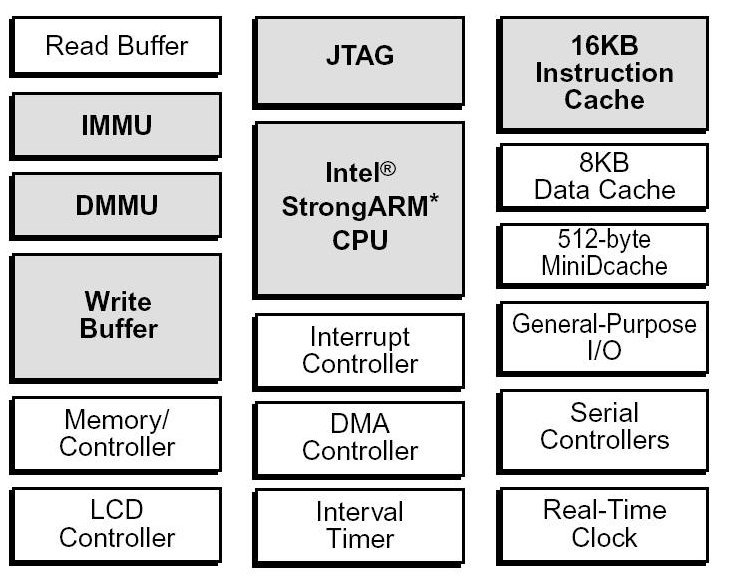
The SA-1110 is a general-purpose, 32-bit RISC microprocessor with a 16 Kbyte instruction cache, an 8 Kbyte write-back data cache, a minicache, a write buffer, a read buffer, and a memory management unit (MMU) combined in a single chip. The SA-1110 is software compatible with the ARM* V4 architecture processor family and can be used with ARM* support chips such as I/O, memory, and video. The core of the SA-1110 is derived from the core of the Intel® StrongARM SA-110 Microprocessor (SA-110), with the following changes:
Reduction in size of the data cache from 16 Kbyte to 8 Kbyte
Addition of a 512-byte mini data cache that allocates data based on MMU settings
Addition of debug support in the form of address and data breakpoints
Addition of a four-entry read buffer to facilitate software-controlled data prefetching
Addition of vector address adjust capability
Addition of a process ID register The logic outside the core and caches is grouped into the following three modules:
Memory and PCMCIA control module (MPCM) Memory interface supporting ROM, Synchronous Mask ROM (SMROM), Flash, DRAM, SDRAM, SRAM, SRAM-like variable latency I/O, and PCMCIA control signals
System control module (SCM) Twenty-eight general-purpose interruptible I/O ports Real-time clock, watchdog, and interval timers Power management controller Interrupt controller Reset controller Two on-chip oscillators for connection to 3.686 MHz and 32.768 kHz crystals
Peripheral control module (PCM) Six-channel DMA controller Gray/color, active/passive LCD controller 16550-compatible UART IrDA serial port (115 Kbps, 4 Mbps) Synchronous serial port (UCB1100, UCB1200, SPI, TI, µWire) Universal serial bus (USB) device controller The instruction set comprises eight basic instruction types:
Two make use of on-chip arithmetic logic unit, barrel shifter, andmultiplier to perform high-speed operations on data in a bank of 16 logical registers (31 physical registers), each 32 bits wide.
Three classes of instructions control data transfer between memory and the registers: one optimized for flexibility of addressing, one for rapid context switching, and one for swapping data.
Two instructions control the flow and privilege level of execution.
One class is used to access the privileged state of the CPU.
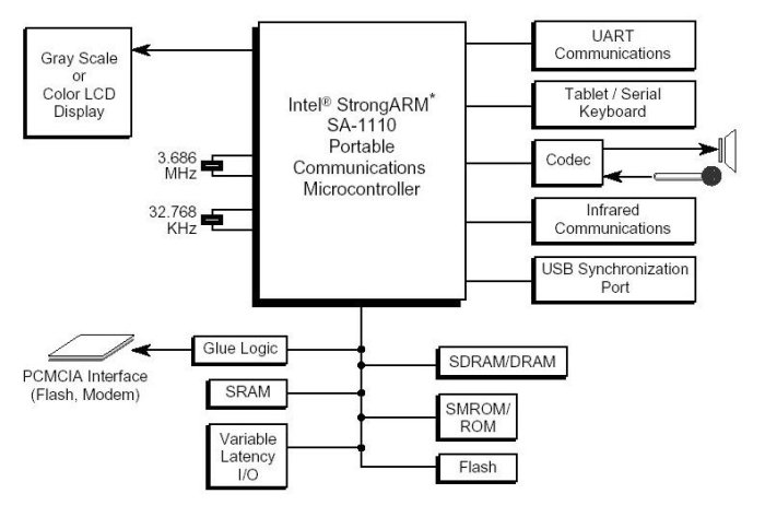
Eine mögliche Anwendung mit SA-1110
The ARM Architecture
The SA-1110 implements the ARM* V4 architecture as defined in the ARM Architecture Reference, 28-July-1995, with the following options:
26-Bit Mode The SA-1110 supports 26-bit mode but all exceptions are initiated in 32-bit mode. The P and D bits do not affect the operation of SA-1110; they are always read as ones and writes to them are ignored.
Coprocessors The SA-1110 supports MCR and MRC access to coprocessor number 15. These instructions are used to access the memory-management, configuration, and cache control registers. In addition, coprocessor 15 provides control for read buffer fills and flushes, and hardware breakpoints. All other coprocessor instructions cause an undefined instruction exception. No support for external coprocessors is provided.
Memory Management Memory management exceptions preserve the base address registers so that no code is required to restore state. Separate translation lookaside buffers (TLBs) are implemented for the instruction and data streams. Each TLB has 32 entries that can each map a segment, a large page, or a small page. The TLB replacement algorithm is round robin. The data TLBs support both the flush-all and flush-single-entry operations, while the instruction TLBs support only the flush-all operation.
Instruction Cache The SA-1110 has a 16 Kbyte instruction cache (Icache) with 32-byte blocks and 32-way associativity. The cache supports the flush-all function. Replacement is round robin within a set. The Icache can be enabled while memory management is disabled. When memory management is disabled, all memory is considered cacheable by the Icache.
Data Cache The SA-1110 has an 8 Kbyte data cache (Dcache) with 32-byte blocks and 32-way associativity. The cache supports the flush-all, flush-entry, and copyback-entry functions. The copyback-all function is not supported in hardware. This function can be provided by software. The cache is read allocate with round-robin replacement. The Dcache has been augmented with a 16-entry, two-way set associative minicache that allocates when the MMU b and c bits are 0 and 1, respectively. This cache is accessed in parallel with the main Dcache. Unlike the main data cache, the minicache implements a least-recently-used (LRU) replacement algorithm. This cache is useful for applications that access large data structures and would normally thrash the main Dcache. Instead, these data structures can be mapped so that they allocate into the minicache and only replace data from the same structure.
Write Buffer The SA-1110 has an eight-entry write buffer with each entry able to contain 1 to 16 bytes. A drain write buffer operation is supported. 1.4.7 Read Buffer The SA-1110 has a four-entry read buffer capable of loading 1, 4, or 8 words of data per entry. This facility permits software to preload data into the buffer for use at a later time without blocking the operation of the processor. Software can flush either a single entry or the entire buffer (four entries). The read buffer is controlled through system control coprocessor 15 and can be enabled for use in user mode.
The SA-1110 consists of the following functional blocks:
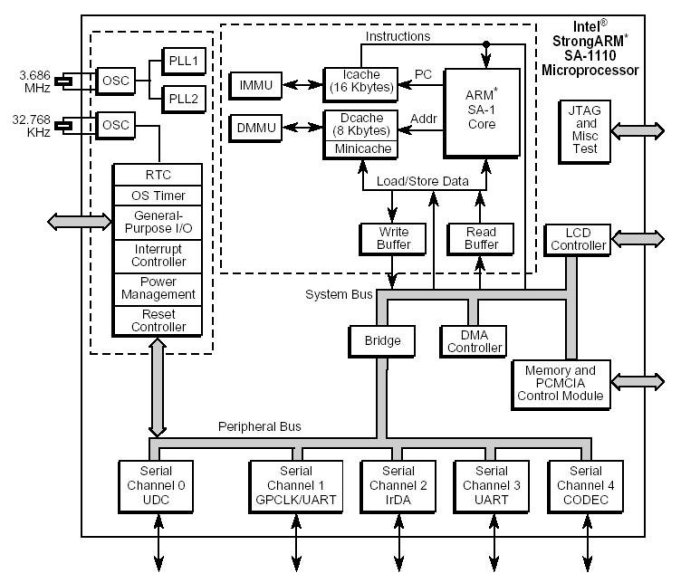
SA-1110 Blockschaltbild
Processing Core The processor is the ARM* SA-1 core with a 16 Kbyte instruction cache (Icache) and 8 Kbyte data cache (Dcache). The instruction (I) and data (D) streams are translated through independent memory-management units (MMUs). Stores are made using a four-line write buffer. The performance of specialized load routines is enhanced with the four-entry read buffer that can be used to prefetch data for use at a later time. A 16-entry minicache provides a smaller and logically separate data cache that can be used to enhance caching performance when dealing with large data structures.
Memory and PCMCIA Control Module The memory and PCMCIA control module (MPCM) supports four banks of fast-page-mode (FPM), extended-data-out (EDO), and/or synchronous DRAM (SDRAM). It also supports up to six banks of static memory: all six banks allow ROM or Flash memory, each with non-burst or burst read timings. Additionally, the lower three static banks support SRAM, the upper three static banks support variable latency I/O devices (with the variable data latency controlled by a shared data ready input), and the lower four static banks support synchronous mask ROM (SMROM). SMROM is supported only on 32-bit data busses. All other dynamic and static memory types and variable latency I/O devices are supported on either 16-bit or 32-bit data busses. Expansion devices are supported through PCMCIA control signals that share the memory bus data and address lines to complete the card interface. Some external glue logic (buffers and transceivers) is necessary to implement the interface. Control is provided to permit two card slots with hot-swap capability.
Peripheral Control Module The peripheral control module (PCM) contains a number of serial control devices, an LCD controller as well as a six-channel DMA controller to provide service to these devices: An LCD controller with support for passive or active displays. A universal serial bus (USB) endpoint controller. A serial controller with supporting 115 Kbps and 4 Mbps IrDA protocols. A 16550-like UART supporting 230 Kbps. A CODEC interface supporting Motorola SPI, National Microwire, TI Synchronous Serial, or the Phillips UCB1100 and UCB1200 protocol
System Control Module The system control module (SCM) is also connected to the peripheral bus. It contains five blocks used for general system functions: A real-time clock (RTC) clocked from an independent 32.768 kHz oscillator. An operating system timer (OST) for general systemtimer functions as well as a watchdog mode. Twenty-eight general-purpose I/Os (GPIO). An interrupt controller. A power-management controller that handles the transitions in and out of sleep and idle modes. A reset controller that handles the various reset sources on the processor.
SA-1110 CPU
The SA-1110 has no external coprocessor bus, so it is not possible to add external coprocessors to this device.
The SA-1110 uses the internal coprocessor designated 15 for control of the on-chip MMU, caches, clocks, and breakpoints. Coprocessor 15 is also used for read-buffer fills and flushes. If a coprocessor other than 15 is used, then the SA-1110 will take the undefined instruction trap. The coprocessor load, store, and data operation instructions also take the undefined instruction trap. Permissions are set so that access to coprocessor 15 is privileged except where protection is programmable with respect to the read buffer operations.
Für eine Firma oder ein Entwicklerteam, das bislang mit dem Intel® StrongARM SA-1110 gearbeitet hat, ergibt sich allerdings ein Problem, da Intel mitteilt, dass dieser chip nicht mehr weiter produziert wird.
Please Note: The Intel® StrongARM SA-1110 has been manufacturer discontinued. As a result, Intel StrongARM SA-1110 processor promotional / support information is no longer available on the web. Options exist for upgrading Intel StrongARM SA-1110 processor-based designs to Intel® PXA255 processor or Intel® PXA26x processor family-based designs.
However, replacement of the Intel StrongARM SA-1110 processor by the Intel PXA255 processor or Intel PXA26x processor family will require varying degrees of engineering design consideration. The Intel PXA255 processor and Intel PXA26x processor family are not pin-for-pin replacements for the Intel StrongARM SA-1110 processor.
Refer to Appendix A of the Intel PXA255 Processor Design Guide, which highlights the process to upgrade an Intel StrongARM SA-1110 design to an Intel PXA255 or Intel PXA26x design. Contact your Intel representative for upgrade assistance if necessary.
Eine mögliche Alternative wird mit der Intel® PXA26x processor family angedeutet. Eine Vorstufe waere die Intel-Familie PXA255, die auch auf der Intel XScale-Architektur basiert (siehe z.B. http://www.xbow.com/Products/Product_pdf_files/Wireless_pdf/6020-0049-02_A_Stargate.pdf ).
While the Intel® PXA260 processor utilizes an identical footprint in a stand alone discreet solution, the Intel® PXA261, PXA262 and PXA263 processors are the first Intel PCA processors based on Intel's Multiple-Chip Product (MCP) packaging technology. This innovative technology utilizes an Intel XScale® technology based processor with integrated peripherals which are "stacked" in a single package with either 16 MegaBytes (Intel PXA261) or 32 MegaBytes (Intel PXA262 and PXA263) of Intel StrataFlash® memory. This enables higher levels of integration and space savings than previous generations of Intel PCA processor standalone products.
Based on Intel XScale® technology, the PXA26x processor family delivers high performance and low power, while providing processing capabilities that allow wireless handsets to respond quickly to performance-intensive applications like MPEG4 video decode, speech and handwriting recognition, and Java* interpretation. Featuring integrated peripherals, the Intel PXA26x processors offer phone and PDA designers expanded functionality, such as an integrated LCD controller with its own Direct Memory Access (DMA) as well as Multi-Media, Secure Digital and CompactFlash (MMC/SD/CF) card support for expandable memory and greater versatility.
A variety of communication ports, including Universal Serial Bus (USB), Infrared (IrDA), I2S and AC'97 audio codec interfaces, high speed Bluetooth** and Baseband interfaces, Universal Asynchronous Receive and Transmit (UART), and Synchronous Serial Port (SSP) enable fast synchronization and communication with other devices.
Manufactured using Intel's 0.18-micron process technology, the integrated Intel StrataFlash® memory offers high value, performance and reliability, and remains the industry's lowest cost-per-bit NOR Flash memory solution featuring 2-bit-per-cell technology.
The Intel PXA26x processor family uses a small 13 x 13 x 1.4 mm package, reducing board space and placement costs. The Intel PXA26x processor family enhances this space savings by using one integrated component instead of multiple discrete Flash and processor components. The Intel PXA26x processor family also provides enhanced scalability within the same envelope, as all derivative configurations utilize the same package and same ball footprint, helping to eliminate the need to redesign a device's main Printed Circuit Board (PCB).
Complementing the Intel PXA26x processor family is a robust software and hardware development environment. Developers have access to a large library of ARM*-compliant applications and tools plus an abundant set of key wireless operating systems and tool chains, including real-time and interactive development systems. Developers can use these resources to build libraries of new feature-rich, industry-leading applications for Intel XScale® technology-based products helping to reduce overall time-to-market.
Finally, Intel delivers Intel® Integrated Performance Primitives (Intel® IPP) for Intel XScale® technology-based processors that helps enable designers to develop applications that can be ported to run on any Intel® PCA processor and the Intel® Flash Data Integrator (Intel® FDI) for Intel StrataFlash® Memory which helps designers enable handheld devices to handle the complex features and demands of Internet storage data. This combination allows highly optimized platforms for wireless handheld devices that incorporate all the benefits of Intel PCA.
Ausführliche Informationen zu dieser CPU findet man auf der PXA270 Entwicklerseite von Intel. Hier nur einige wichtige Eigenschaften für eine erste Einordnung dieser CPU.
Trotz aller neuen Eigenschaften hat Intel versucht, diese neue CPU kompaibel zur vorausgehenden stronARM-Architektur zu halten. Es heisst:
The Intel XScale® core is an ARM V5TE compliant microprocessor. It has been designed for high performance and low-power; leading the industry in mW/MIPs. The core is not intended to be delivered as a stand alone product but as a building block for an ASSP (Application Specific Standard Product) with embedded markets such as handheld devices, networking, storage, remote access servers, etc. The Intel XScale® core incorporates an extensive list of architecture features that allows it to achieve high performance. This rich feature set allows programmers to select the appropriate features that obtains the best performance for their application. Many of the architectural features added to the Intel XScale® core help hide memory latency which often is a serious impediment to high performance processors. This includes:
the ability to continue instruction execution even while the data cache is retrieving data from external memory.
a write buffer.
write-back caching.
various data cache allocation policies which can be configured different for each application.
and cache locking.
All these features improve the efficiency of the memory bus external to the core. The Intel XScale® core has been equipped to efficiently handle audio processing through the support of 16-bit data types and 16-bit operations. These audio coding enhancements center around multiply and accumulate operations which accelerate many of the audio filter operations.
Speziell zur ARM-Kompatibilität heisst es nochmals:
ARM Version 5 (V5) Architecture added floating point instructions to ARM Version 4. The Intel XScale® core implements the integer instruction set architecture of ARM V5, but does not provide hardware support of the floating point instructions. The Intel XScale® core provides the Thumb instruction set (ARM V5T) and the ARM V5E DSP extensions. Backward compatibility with StrongARM* products is maintained for user-mode applications. Operating systems may require modifications to match the specific hardware features of the Intel XScale® core and to take advantage of the performance enhancements added.
Ein Blockchaltbild zur PXA270-CPU ist das folgende:

Intel PXA720
Eine komprimierte Liste aller wichtigen Eigenschaften ist die folgende:
Intel XScale® Technology Highly scalable core up to 520 MHz
Embedded Packaging 23x23 mm with 1.0 mm ball pitch 13x13 mm with 0.5 mm ball pitch also available
Extended Temperature Range -40°C to 85°C ambient temperature range available
Product Life Cycle Anticipated five-year life cycle1
Incredible Multimedia Familiar Intel® Wireless MMX" technology instructions designed for high-performance multimedia, 3-D games and advanced video
Advanced Camera Interface Intel® Quick Capture technology supports 4+ megapixel cameras for capturing digital images, video and low-power, real-time previews
Enhanced LCD Controller Dual-panel LCD with up to 24-bit color. Hardware color space conversion with 256 KB of on-chip SRAM for faster video. Two overlays reduce LCD bandwidth. Integrated Intel Quick Capture technology enables fast video preview
Reduced Power Consumption Wireless Intel SpeedStep® Power Manager technology with five low-power modes can change frequency and voltage dynamically. Wireless Intel SpeedStep Power Manager software enables built-in, intelligent power management
Fast Access to Wireless Data Intel® Mobile Scalable Link provides up to 416 Mbps link between communications and applications processors
Large Peripheral Set USB Host/Client USB OTG 4-bit SD I/O MMC/SDCard Memory Stick USIM card interface Keypad controller PCMCIA/CF ICP
Memory Interface 100 MHz memory bus supports a variety of 1.8 V, 2.5 V, 3.0 V and 3.3 V memory
Eine noch radikaleres Konzept für eine kleine und äusserst leistungsarme CPU wurde mit dem MSP430 von Texas Instruments realisiert.
Texas Instruments schreibt dazu:
The MSP430 employs a von-Neumann architecture, therefore, all memory and peripherals are in one address space.
The MSP430 devices constitute a family of ultralow-power, 16-bit RISC microcontrollers with an advanced architecture and rich peripheral set. The architecture uses advanced timing and design features, as well as a highly orthogonal structure to deliver a processor that is both powerful and flexible. The MSP430 consumes less than 400 microA in active mode operating at 1 MHz in a typical 3-V system and can wake up from a <2-microA standby mode to fully synchronized operation in less than 6 micros. These exceptionally low current requirements, combined with the fast wake-up time, enable a user to build a system with minimum current consumption and maximum battery life.
Additionally, the MSP430 family has an abundant mix of peripherals and memory sizes enabling true system-on-a-chip designs. The peripherals include a 14-bit A/D, slope A/D, multiple timers (some with capture/compare registers and PWM output capability), LCD driver, on-chip clock generation, H/W multiplier, USART, Watchdog Timer, GPIO, and others.
Hier ein Blockschaltbild:

TI MSP430
Zum eigentlichen CPU-Kern heisst es:
The processing unit is based on a consistent and orthogonally-designed CPU and instruction set. This design structure results in a RISC-like architecture, highly transparent to the application development and is distinguished due to ease of programming. All operations other than program-flow instructions are consequently performed as register operations in conjunction with seven addressing modes for source and four modes for destination operand.
CPU Sixteen registers are located inside the CPU, providing reduced instruction execution time. This reduces a register-register operation execution time to one cycle of the processor frequency. Four of the registers are reserved for special use as a program counter, a stack pointer, a status register and a constant generator. The remaining registers are available as general-purpose registers. Peripherals are connected to the CPU using a data address and control bus and can be handled easily with all instructions for memory manipulation.

TI MSP430 Registers
The instruction set for this register-register architecture provides a powerful and easy-to-use assembler language. The instruction set consists of 51 instructions with three formats and seven addressing modes.
Ein wichiges Einsatzgebiet der MSP430-CPU sind z.B. drahtlose Sensornetzwerke. Hier ein illustrativer Artikel vom Computer Science Department der University of Californiax at Berkeley (siehe: http://webs.cs.berkeley.edu/papers/hotchips-2004-polastre.txt ):
The Mote Revolution: Low Power Wireless Sensor Network Devices
Joseph Polastre, Robert Szewczyk, Cory Sharp, and David Culler {polastre, szewczyk, cssharp, culler} @ cs.berkeley.edu
A family of low power wireless sensor network devices have been built to enable research and deployments. The devices have featured commercial off the shelf (COTS) components integrated together on a platform commonly referred to as a "mote" [2,4]. Motes have been used to evaluate wireless sensor network algorithms as well as for environmental monitoring and object tracking deployments. Miniature wireless devices are ideal for high density long term deployments in areas otherwise unsuitable for wired connections or passive devices. We describe the design and implementation of a next generation sensor mote that utilizes emerging hardware, miniature sensors, and new standards to achieve high data rate, extremely low power operation for monitoring applications [6]. Fine grained power management is essential for wireless sensor network applications that run for months (such as an organism's breeding season) or years (in HVAC or structural monitoring).
Low power operation is achieved not only through selection of efficient hardware, but also through duty cycling that hardware; care must be taken to minimize common operations. From experience building a family of wireless sensor nodes, or "motes" (see Table 1 attached), we have observed the primary operations in low duty cycle operation are sleep, wakeup, and run (in that order). One cycle of sleep, wakeup, and run is typically the cost of acquiring a single set of sensor samples. For the majority of the time the node is sleeping. While asleep, the microcontroller must maintain its state (typically in RAM) while consuming little power and shutting down or disconnecting all peripherals including the radio. For Telos, our newest and lowest power mote to date, we chose the Texas Instruments MSP430 microcontroller (specifically the F1611 although our device is backwards compatible with the F149) [7]. The MSP430 consumes only 2 microwatts in sleep mode while maintaining RAM. Other microcontroller features include direct memory access, supply voltage supervisor, and hardware implementations of SPI, USART, and I2C. In low power applications, it is important to run all auxiliary hardware components (ADC, DMA, bus operations) from a low speed (often 32kHz) external clock so that the microcontroller oscillator core can be shut down for additional power savings.
During the wakeup phase, the mote must start the core of the microcontroller for processing. It may also start the radio and sensors for sampling. The MSP430 can wake up in under 6 microseconds. Short deterministic wakeups are important for two types of low power communication--low power listening and scheduled communication. Low power listening periodically samples the radio channel for activity. If no activity is found, the node returns to sleep. Low power listening does not require time synchronization, instead the duty cycle is dependent on the network traffic and the startup time of the microcontroller. Scheduled communication performs synchronization with the network and wakes up at specified intervals for communication. Minimizing the active time with a scheduled communication scheme requires minimizing the non-deterministic portion of the startup time.
The active or running portion of the mote's duty cycle is typically an extremely small portion of the overall mote lifetime. Accordingly, we first focused on selecting components with low sleep profiles and fast wakeups. When the node is active, it is important to be able to control the power to each of the external peripherals. Keeping the active time small requires a low power yet fast microcontroller. The MSP430 is a 16-bit microcontroller running at 4MHz with only 0.5 milliwatts active current consumption. We chose to couple the MSP430 with the CC2420 [1] IEEE 802.15.4 [5] compliant radio to enable standardized network communication between different hardware devices. Previous to IEEE 802.15.4, motes used radios with custom protocol implementations. Now with IEEE 802.15.4, sensor networks may grow to very large networks through interoperating devices with a standardized (and FCC certifiable) radio and MAC protocol layer. The CC2420 is a low power transceiver (17mA receive/19mA transmit) at 250kbps using O-QPSK. The startup time of the radio is approximately 1ms to calibrate an external 16MHz oscillator. We found that radios could either be self-clocked or externally clocked by the microcontroller. Either option requires a highly accurate oscillator on-board. We chose not to use an external high speed oscillator with the microcontroller and instead allow the microcontroller to sleep while the radio starts up, processes, or while sensors are acquiring data.
For robustness, we chose to package a suite of sensors integrated onto the mote. Telos uses USB for power, programming, and communication with a host computer. Upon disconnection from USB, the mote runs on batteries that are isolated from the USB circuitry to prevent current leakage. An integrated antenna is robust against handling and environmental packaging; it is augmented with an external antenna connector for flexibility. Of importance to consumers, integrating a complete solution on to a single mote significantly reduces cost and eliminates the need for support hardware found in previous generations of motes (programming boards, interface boards, and sensor boards).
All of the components in the system--the microcontroller, radio, flash, and sensors--operate down to 1.8V. By running at 1.8V for the life of a mote, it can double its lifetime by using half the power of running at 3.6V. With an LDO regulator and a small number of discrete components, the mote can utilize live almost twice as long on the exact same battery as previous mote generations.
This collection of features has been integrated to create the highest data rate, lowest power mote to date. It lowers the barrier of entry to using wireless sensor networks for commercial applications by lowering cost, using standards such as USB and IEEE 802.15.4, and leveraging open source tools such as gcc and TinyOS [8].
References:
[1] Chipcon AS. CC2420 2.4GHz IEEE 802.15.4 compliant RF Transceiver. November 2003. http://www.chipcon.com
[2] Jason Hill, Robert Szewczyk, Alec Woo, Seth Hollar, David Culler, Kristofer Pister. System Architecture Directions for Networked Sensors. ASPLOS 2000: 93-104.
[3] Jason Hill, David Culler. Mica: A Wireless Platform for Deeply Embedded Networks. IEEE Micro 22(6): 12-24 (2002).
[4] Jason Hill. System Architecture for Wireless Sensor Networks. PhD Thesis, University of California, Berkeley, 2003.
[5] IEEE Standard for Information Technology: 802.15.4: Wireless Medium Access Control and Physical Layer Specifications for Low-Rate Wireless Personal Area Networks. 2003.
[6] Alan Mainwaring, Joseph Polastre, Robert Szewczyk, David Culler, John Anderson. Wireless sensor networks for habitat monitoring. WSNA 2002: 88-97.
[7] Texas Instruments. MSP430 Microcontroller: F1611 User's Guide. 2004. http://www.ti.com.
[8] TinyOS: An Operating System for the Wireless Sensor Regime. http://www.tinyos.net.
Eine gute Quelle für Entwicklungsboards und Software für die MSP430-CPU ist Softbaugh.
Welche Eigenschaften sollten CPUs für mobile eingebettete Systeme gegenüber normalen CPUs auszeichnen?
Welches sind die heute wichtigsten CPUs für eingebetete und speziell mobile eingebettete Systeme?
Nennen Sie wichtige Eigenschaften dieser neuen CPUs?