
|
|
II-INFORMATIK3 WS04
|
Der vorausgehende Versuch, die Funktionsweise der Intel CPUs aufgrund der offiziell verfügbaren Dokumente zu rekonstruieren, war nicht vollständig erfolgreich. Die Dokumente erwiessen sich als sehr komplex und zugleich als nicht vollständig. Dies wurde auch durch ausgewiessene sekundäre Fachliteratur bestätigt. Abschliessend soll hier dennoch nochmals auf die Gesamtarchitektur eingegangen werden speziell unter der Rücksicht der Befehlsverarbeitung. Wir benutzen weiterhin die offiziellen Intel-Dokumente (siehe Literatur-Liste) ergänzt um das Buch von [BREY 2003].
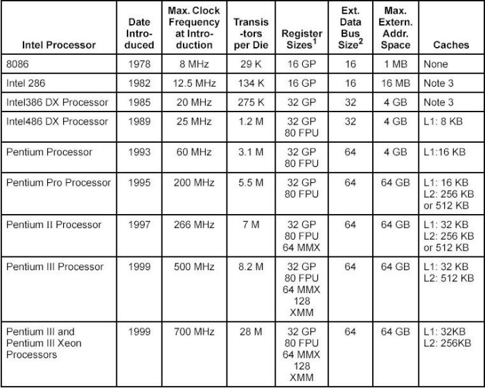
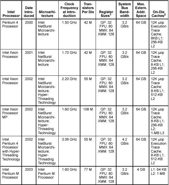
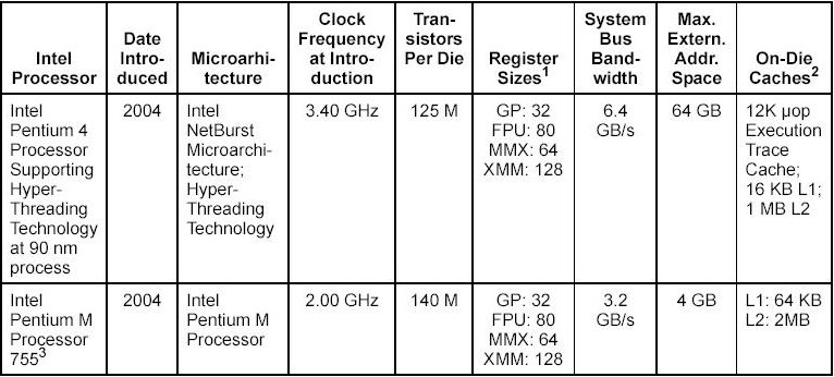
Einen Überblick über die Entwicklung der 16-, 32- und 64-Bit CPUs von Intel findet sich in im Software Developers Manual Vol.1, 2-1 ff, sowie an verschiedenen stellen auf den Intel-Webseiten, speziell im Bereich Intel Museum.
|
Zeit |
CPU-Typ |
Eigenschaften |
|---|---|---|
|
1971 |
4004 |
4 Bit, 45 Instruktionen, 50 KIPs |
|
1971 |
4040 |
schneller |
|
1972 |
8008 |
8 Bit, 48 Instruktionen, 50 KIPs, adressiert 16 KB memory |
|
1974 |
8080 |
8 Bit, 500 KIPs, adressiert 64 KB memory |
|
1977 |
8085 |
8 Bit, 246 Instruktionen, 769.2 KIPs |
|
1978 |
8086 |
16 Bit Daten, 20.000 Instruktionen, 2.5 MIPs, adressiert 1 MB memory, 4-6 Byte Befehlscache, mehr interne Register |
|
1979 |
8088 |
8 Bit Daten, 20.000 Instruktionen, 2.5 MIPs, adressiert 1 MB memory, 4-6 Byte Befehlscache, mehr interne Register |
|
1982
|
80286
|
16 Bit Daten, adressiert 16 MB Memory, 4.0 MIPs. The Intel 286 processor introduced protected mode operation into the IA-32 architecture. Protected mode uses the segment register content as selectors or pointers into descriptor tables. Descriptors provide 24-bit base addresses with a physical memory size of up to 16 MBytes, support for virtual memory management on a segment swapping basis, and a number of protection mechanisms. These mechanisms include: ->Segment limit checking ->Read-only and execute-only segment options ->Four privilege levels. |
|
Zeit |
CPU-Typ |
Eigenschaften |
|---|---|---|
|
1985/6 |
80386
|
32 Bit Daten und Adressen, addressiert 4 GB Memory, abwärts kompatibel bis 8086
The Intel386 processor was the first 32-bit processor in the IA-32 architecture family. It introduced 32-bit registers for use both to hold operands and for addressing. The lower half of each 32-bit Intel386 register retains the properties of the 16-bit registers of earlier generations, permitting backward compatibility. The processor also provides a virtual-8086 mode that allows for even greater efficiency when executing programs created for 8086/8088 processors. In addition, the Intel386 processor has support for: ->A 32-bit address bus that supports up to 4-GBytes of physical memory ->A segmented-memory model and a flat1 memory model ->Paging, with a fixed 4-KByte page size providing a method for virtual memory management ->Support for parallel stages |
|
|
80386SX |
16 Bit Daten, 24 Bit Adressen |
|
|
80386SL |
16 Bit Daten, 25 Bit Adressen |
|
|
80386SLC |
16 Bit Daten, 25 Bit Adressen, interner 1KB Cache |
|
|
80386EX |
16 Bit Daten, 26 Bit Adressen, 24 I/O Daten, embedded version |
|
1989
|
80486(DX2/DX4) |
Mit numerischem Ko-prozessor und 8 KB Cache (16 KB Cache), 50% der Befehle konnten in 1 Zyklus abgearbeitet werden anstatt in 2 Zyklen, bei 50 MHz ergab dies bei den 1 Zyklus-Befehlen 50 MIPs
The Intel486" processor added more parallel execution capability by expanding the Intel386 processor's instruction decode and execution units into five pipelined stages. Each each stage operates in parallel with the others on up to five instructions in different stages of execution. In addition, the processor added: ->An 8-KByte on-chip first-level cache that increased the percent of instructions that could execute at the scalar rate of one per clock ->An integrated x87 FPU ->Power saving and system management capabilities |
|
1993
|
80586 = P5, Pentium I |
Ähnlich wie 80486, 64 Bit Datenbus, 110 - 300 MIPs, 8 KB Daten-Cache, 8 KB Instruktions-Cache, spezielle Multimedia Befehle (MMX) The introduction of the Intel Pentium processor added a second execution pipeline to achieve superscalar performance (two pipelines, known as u and v, together can execute two instructions per clock). The on-chip first-level cache doubled, with 8 KBytes devoted to code and another 8 KBytes devoted to data. The data cache uses the MESI protocol to support more efficient writeback cache in addition to the write-through cache previously used by the Intel486 processor. Branch prediction with an on-chip branch table was added to increase performance in looping constructs. In addition, the processor added: ->Extensions to make the virtual-8086 mode more efficient and allow for 4-MByte as well as 4-KByte pages ->Internal data paths of 128 and 256 bits add speed to internal data transfers ->Burstable external data bus was increased to 64 bits " An APIC to support systems with multiple processors ->A dual processor mode to support glueless two processor systems A subsequent stepping of the Pentium family introduced Intel MMX -technology (the Pentium Processor with MMX technology). Intel MMX technology uses the single-instruction, multipledata (SIMD) execution model to perform parallel computations on packed integer data contained in 64-bit registers. |
|
|
|
|
The P6 family of processors was based on a superscalar microarchitecture that set new performance standards. One of the goals in the design of the P6 family microarchitecture was to exceed the performance of the Pentium processor significantly while using the same 0.6-micrometer, four-layer, metal BICMOS manufacturing process. Members of this family include:
->Intel Pentium Pro processor
->Intel Pentium II processor
->Intel Pentium® II Xeon-processor
->Intel Celeron® processor
->Intel Pentium III processor
->Intel Pentium® III Xeon" processor
|
Zeit |
CPU-Typ |
Eigenschaften |
|---|---|---|
|
1995
|
Pentium Pro = P6 |
64 Bit Datenbus, 4 G Memory, 16K L1 (= 8K Daten + 8K Instruktionen) + 256K L2 Cache, drei Integer Prozessoren, Fliesskomma-Ko-prozessor, 32-36 Bit Adressen
The Intel Pentium Pro processor is three-way superscalar. Using parallel processing techniques, the processor is able on average to decode, dispatch, and complete execution of (retire) three instructions per clock cycle. The Pentium Pro introduced the dynamic execution (microdata flow analysis, out-of-order execution, superior branch prediction, and speculative execution) in a superscalar implementation. The processor was further enhanced by its caches. It has the same two on-chip 8-KByte 1st-Level caches as the Pentium processor and an additional 256 KByte Level 2 cache in the same package as the processor. |
|
1997
|
Pentium II (P6 Architektur) |
wie PentiumPro, zusätzlich 64 G Memory, 32 K L1 + 512K/ 1M L2 Cache
The Intel Pentium II processor added Intel MMX Technology to the P6 family processors along with new packaging and several hardware enhancements. The processor core is packaged in the single edge contact cartridge (SECC). The Level l data and instruction caches were enlarged to 16 KBytes each, and Level 2 cache sizes of 256 KBytes, 512 KBytes, and 1 MByte are supported. A half-clock speed backside bus connects the Level 2 cache to the processor. Multiple low-power states such as AutoHALT, Stop-Grant, Sleep, and Deep Sleep are supported to conserve power when idling. |
|
1998
|
Pentium II Xeon (P6 Architektur) |
wie PentiumPro, zusätzlich 64 G Memory, 32 K L1 + 512K/ 1M/ 2M L2 Cache
The Pentium II Xeon processor combined the premium characteristics of previous generations of Intel processors. This includes: 4-way, 8-way (and up) scalability and a 2 MByte 2nd-Level cache running on a full-clock speed backside bus. |
|
1999
|
Pentium III (P6 Architektur) |
wie PentiumPro, zusätzlich 64 G Memory, 32 K L1 + 256K /512K L2 Cache, SDRAM
The Intel Pentium III processor introduced the Streaming SIMD Extensions (SSE) to the IA-32 architecture. SSE extensions expand the SIMD execution model introduced with the Intel MMX technology by providing a new set of 128-bit registers and the ability to perform SIMD operations on packed single-precision floating-point values. |
|
2000/2004
|
Pentium IV (P6 Architektur) |
wie PentiumPro, zusätzlich 64 G Memory, 8 K L1 + 256K /512K L2 Cache, Rambus-Technologie
The Intel Pentium 4 processor is based on Intel NetBurst® microarchitecture. It also introduced the following major feature sets: ->Streaming SIMD Extensions 2 (SSE2)->Streaming SIMD Extensions 3 (SSE3) |
|
2001/2004 |
Intel Xeon |
The Intel Xeon processor is also based on the Intel NetBurst microarchitecture. As a family, this group of IA-32 processors is designed for use in multi-processor server systems and high-performance workstations. |
|
2003/2004 |
Intel Pentium M |
The Intel Pentium M processor family is a high performance, low power mobile processor family with microarchitectural enhancements over previous generations of Intel mobile processors. This family is designed for extending battery life and seamless integration with platform innovations that enable new usage models (such as extended mobility, ultra thin form-factors, and integrated wireless networking). |
This basic execution environment is used jointly by the application programs and the operating system or executive running on the processor.
Address Space. Any task or program running on an IA-32 processor can address a linear address space of up to 4 GBytes (232 bytes) and a physical address space of up to 64 GBytes (236 bytes).
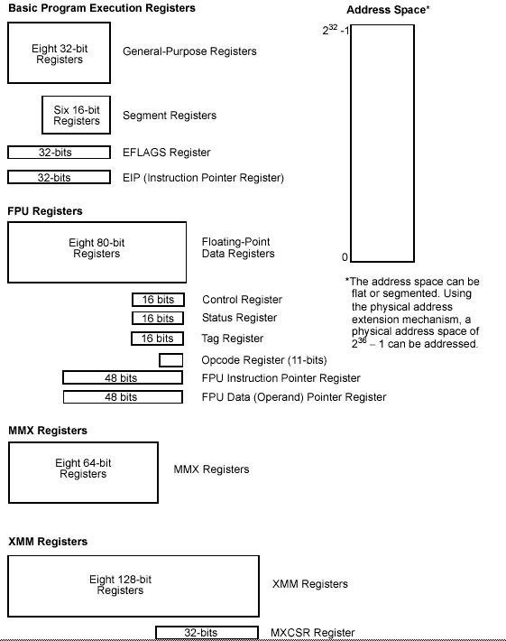
Basic program execution registers. The eight general-purpose registers, the six segment registers, the EFLAGS register, and the EIP (instruction pointer) register comprise a basic execution environment in which to execute a set of general-purpose instructions. These instructions perform basic integer arithmetic on byte, word, and doubleword integers, handle program flow control, operate on bit and byte strings, and address memory.
x87 FPU registers. The eight x87 FPU data registers, the x87 FPU control register, the status register, the x87 FPU instruction pointer register, the x87 FPU operand (data) pointer register, the x87 FPU tag register, and the x87 FPU opcode register provide an execution environment for operating on single-precision, double-precision, and double extendedprecision floating-point values, word integers, doubleword integers, and quadword integers, and binary coded decimal (BCD) values.
MMX-registers. The eight MMX registers support execution of single-instruction, multiple-data (SIMD) operations on 64-bit packed byte, word, and doubleword integers.
XMM-registers. The eight XMM data registers and the MXCSR register support execution of SIMD operations on 128-bit packed single-precision and double-precision floating-point values and on 128-bit packed byte, word, doubleword, and quadword integers.
Stack. To support procedure or subroutine calls and the passing of parameters between procedures or subroutines, a stack and stack management resources are included in the execution environment. The stack is located in memory.
In addition to the resources provided in the basic execution environment, the IA-32 architecture provides the following system resources as part of its system-level architecture. They provide extensive support for operating-system and system-development software. Except for the I/O ports, the system resources are described in detail in the IA-32 Intel Architecture Software Developer s Manual, Volume 3: System Programming Guide.
I/O Ports. The IA-32 architecture supports a transfers of data to and from input/output (I/O) ports.
Control registers. The five control registers (CR0 through CR4) determine the operating mode of the processor and the characteristics of the currently executing task.
Memory management registers. The GDTR, IDTR, task register, and LDTR specify the locations of data structures used in protected mode memory management.
Debug registers. The debug registers (DR0 through DR7) control and allow monitoring of the processor s debugging operations.
Memory type range registers (MTRRs). The MTRRs are used to assign memory types to regions of memory.
Machine specific registers (MSRs). The processor provides a variety of machine specific registers that are used to control and report on processor performance. Virtually all MSRs handle system related functions and are not accessible to an application program. One exception to this rule is the time-stamp counter.
Machine check registers. The machine check registers consist of a set of control, status, and error-reporting MSRs that are used to detect and report on hardware (machine) errors.
Performance monitoring counters. The performance monitoring counters allow processor performance events to be monitored.
Beginning with the Pentium II and Pentium with Intel MMX technology processor families, four extensions have been introduced into the IA-32 architecture to permit IA-32 processors to perform single-instruction multiple-data (SIMD) operations. These extensions include the MMX technology, SSE extensions, SSE2 extensions, and SSE3 extensions. Each of these extensions provides a group of instructions that perform SIMD operations on packed integer and/or packed floating-point data elements contained in the 64-bit MMX or the 128-bit XMM registers. Figure 2-3 shows a summary of the various SIMD extensions (MMX technology, SSE, SSE2, and SSE3), the data types they operate on, and how the data types are packed into MMX and XMM registers.
The Intel MMX technology was introduced in the Pentium II and Pentium with MMX technology processor families. MMX instructions perform SIMD operations on packed byte, word, or doubleword integers located in MMX registers. These instructions are useful in applications that operate on integer arrays and streams of integer data that lend themselves to SIMD processing.
SSE extensions were introduced in the Pentium III processor family. SSE instructions operate on packed single-precision floating-point values contained in XMM registers and on packed integers contained in MMX registers. Several SSE instructions provide state management, cache control, and memory ordering operations. Other SSE instructions are targeted at applications that operate on arrays of single-precision floating-point data elements (3-D geometry, 3-D rendering, and video encoding and decoding applications). SSE2 extensions were introduced in Pentium 4 and Intel Xeon processors.
SSE2 instructions operate on packed double-precision floating-point values contained in XMM registers and on packed integers contained in MMX and XMM registers. SSE2 integer instructions extend IA-32 SIMD operations by adding new 128-bit SIMD integer operations and by expanding existing 64-bit SIMD integer operations to 128-bit XMM capability. SSE2 instructions also provide new cache control and memory ordering operations.
SSE3 extensions were also introduced with the Pentium 4 processor supporting Hyper- Threading Technology (built on 90 nm process technology). SSE3 offers 13 instructions that accelerate performance of Streaming SIMD Extensions technology, Streaming SIMD Extensions 2 technology, and x87-FP math capabilities.

MMX instructions move 64-bit packed data types (packed bytes, packed words, or packed doublewords) and the quadword data type between MMX registers and memory or between MMX registers in 64-bit blocks. However, when performing arithmetic or logical operations on the packed data types, MMX instructions operate in parallel on the individual bytes, words, or doublewords contained in MMX registers.
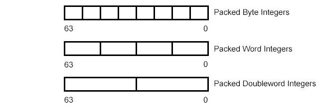
MMX technology uses the single instruction, multiple data (SIMD) technique for performing arithmetic and logical operations on bytes, words, or doublewords packed into MMX registers. For example, the PADDSW instruction adds 4 signed word integers from one source operand to 4 signed word integers in a second source operand and stores 4 word integer results in a destination operand. This SIMD technique speeds up software performance by allowing the same operation to be carried out on multiple data elements in parallel. MMX technology supports parallel operations on byte, word, and doubleword data elements when contained in MMX registers.

Allgemein heisst es zur P6-Architektur: "The microarchitecture is a three-way superscalar, pipelined architecture. Three-way superscalar means that by using parallel processing techniques, the processor is able on average to decode, dispatch, and complete execution of (retire) three instructions per clock cycle. To handle this level of instruction throughput, the P6 processor family uses a decoupled, 12-stage superpipeline that supports out-of-order instruction execution".
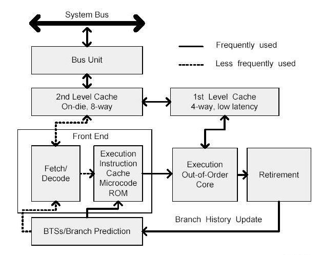
The Level 1 cache provides an 8-KByte instruction cache and an 8-KByte data cache, both closely coupled to the pipeline. The Level 2 cache provides 256-KByte, 512-KByte, or 1-MByte static RAM that is coupled to the core processor through a full clock-speed 64-bit cache bus.
The Level 1 cache provides an 8-KByte instruction cache and an 8-KByte data cache, both closely coupled to the pipeline. The Level 2 cache provides 256-KByte, 512-KByte, or 1-MByte static RAM that is coupled to the core processor through a full clock-speed 64-bit cache bus.
Deep branch prediction allows the processor to decode instructions beyond branches to keep the instruction pipeline full. The P6 processor family implements highly optimized branch prediction algorithms to predict the direction of the instruction.
Dynamic data flow analysis requires real-time analysis of the flow of data through the processor to determine dependencies and to detect opportunities for out-of-order instruction execution. The out-of-order execution core can monitor many instructions and execute these instructions in the order that best optimizes the use of the processor s multiple execution units, while maintaining the data integrity.
Speculative execution refers to the processor's ability to execute instructions that lie beyond a conditional branch that has not yet been resolved, and ultimately to commit the results in the order of the original instruction stream. To make speculative execution possible, the P6 processor microarchitecture decouples the dispatch and execution of instructions from the commitment of results. The processor s out-of-order execution core uses data-flow analysis to execute all available instructions in the instruction pool and store the results in temporary registers. The retirement unit then linearly searches the instruction pool for completed instructions that no longer have data dependencies with other instructions or unresolved branch predictions. When completed instructions are found, the retirement unit commits the results of these instructions to memory and/or the IA-32 registers (the processor s eight general-purpose registers and eight x87 FPU data registers) in the order they were originally issued and retires the instructions from the instruction pool.
The front end supplies instructions in program order to the out-of-order execution core. It performs a number of functions:
Prefetches IA-32 instructions that are likely to be executed
Fetches instructions that have not already been prefetched
Decodes IA-32 instructions into micro-operations
Generates microcode for complex instructions and special-purpose code
Delivers decoded instructions from the execution trace cache
Predicts branches using highly advanced algorithm
The pipeline is designed to address common problems in high-speed, pipelined microprocessors. Two of these problems contribute to major sources of delays:
time to decode instructions fetched from the target
wasted decode bandwidth due to branches or branch target in the middle of cache lines
The operation of the pipeline s trace cache addresses these issues. Instructions are constantly being fetched and decoded by the translation engine (part of the fetch/decode logic) and built into sequences of µops called traces. At any time, multiple traces (representing prefetched branches) are being stored in the trace cache. The trace cache is searched for the instruction that follows the active branch. If the instruction also appears as the first instruction in a pre-fetched branch, the fetch and decode of instructions from the memory hierarchy ceases and the prefetched branch becomes the new source of instructions.
The trace cache and the translation engine have cooperating branch prediction hardware. Branch targets are predicted based on their linear addresses using branch target buffers (BTBs) and fetched as soon as possible.
The out-of-order execution core s ability to execute instructions out of order is a key factor in enabling parallelism. This feature enables the processor to reorder instructions so that if one µop is delayed, other µops may proceed around it. The processor employs several buffers to smooth the flow of µops. The core is designed to facilitate parallel execution. It can dispatch up to six µops per cycle (this exceeds trace cache and retirement µop bandwidth). Most pipelines can start executing a new µop every cycle, so several instructions can be in flight at a time for each pipeline. A number of arithmetic logical unit (ALU) instructions can start at two per cycle; many floating-point instructions can start once every two cycles.
The retirement unit receives the results of the executed µops from the out-of-order execution core and processes the results so that the architectural state updates according to the original program order. When a µop completes and writes its result, it is retired. Up to three µops may be retired per cycle. The Reorder Buffer (ROB) is the unit in the processor which buffers completed µops, updates the architectural state in order, and manages the ordering of exceptions.
The retirement section also keeps track of branches and sends updated branch target information to the BTB. The BTB then purges pre-fetched traces that are no longer needed.
Hyper-Threading (HT) Technology was developed to improve the performance of IA-32 processors when executing multi-threaded operating system and application code or single-threaded applications under multi-tasking environments. The technology enables a single physical processor to execute two or more separate code streams (threads) concurrently.
Architecturally, an IA-32 processor that supports HT Technology consists of two or more logical processors, each of which has its own IA-32 architectural state. Each logical processor consists of a full set of IA-32 data registers, segment registers, control registers, debug registers and most of the MSRs. Each also has its own advanced programmable interrupt controller (APIC).
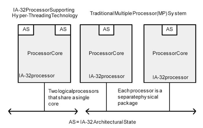
Unlike a traditional MP system configuration that uses two or more separate physical IA-32 processors, the logical processors in an IA-32 processor supporting HT Technology share the core resources of the physical processor. This includes the execution engine and the system bus interface. After power up and initialization, each logical processor can be independently directed to execute a specified thread, interrupted, or halted.
HT Technology leverages the process and thread-level parallelism found in contemporary operating systems and high-performance applications by providing two or more logical processors INTRODUCTION TO THE IA-32 INTEL ARCHITECTURE on a single chip. This configuration allows two or more threads3 to be executed simultaneously on each a physical processor. Each logical processor executes instructions from an application thread using the resources in the processor core. The core executes these threads concurrently, using out-of-order instruction scheduling to maximize the use of execution units during each clock cycle.
Was sind die wichtigsten Eigenschaften, die seit 19971 an den Intel-CPUs verändert wurden?
Wie wirken diese sich auf die Leistung der CPU aus?
Worin genau besteht die Multimedia-Erweiterung der IA32-Architektur?
Worin besteht die superskalare Pipeline-Struktur der IA32-CPUs? Auf welche Weise kann sie die Leistng steigern?
Was ist Hyperthreading und wodurch kann es eine Leistungssteigerng herbeiführen?